eISBN: 978-1-78262-233-8
From Book Series: Energy and Environment Series
CHAPTER 1
Photoelectrochemistry: From Basic Principles to Photocatalysis
Laurence M.
Peter*a
a
Department of Chemistry, University of Bath, Bath BA2 7AY, United Kingdom.
E-mail: l.m.peter@bath.ac.uk
Semiconductor photoelectrochemistry experienced a renaissance stimulated by the development of mesoporous dye-sensitized solar cells following the 1991 Nature paper of O'Regan and Grätzel. The resulting move away from well-defined single crystal bulk materials to high surface area nanostructured electrodes opened a new field of research, and many of the ideas that had been developed for bulk semiconductor electrodes required re-examination in view of the very different length scales. Nanostructured semiconductor electrodes are now also being utilized for light-driven water splitting and environmental remediation. This historical development has resulted in a convergence of the fields of semiconductor photoelectrochemistry and photocatalysis at semiconductor particles. The objective of this chapter is to review the basic ideas that were developed originally to understand the photoelectrochemical behaviour of bulk semiconductors and to see how these ideas need to be modified when considering nanostructured semiconductor electrodes and dispersed colloidal systems.
1.1 Introduction
The foundations of semiconductor photoelectrochemistry were laid by Gerischer,1 Pleskov, Memming,2 Bard3 and others in the 1960s. Several authoritative texts are available that summarize the basic concepts.2,4–6 At this time, the physics and chemistry of light-driven reactions at semiconductor surfaces were studied extensively using well-defined bulk monocrystalline materials. Interest in semiconductor photoelectrochemistry became more widespread following the 1973 oil crisis, which stimulated an urgent search for alternative energy technologies. During this period, several efficient liquid-junction solar cells were developed that utilized (mainly single crystal) semiconductors in contact with redox electrolytes.7 Examples of materials that were studied include CdS, CdSe, GaAs, GaP, InP, WSe2 and MoSe2 (see Morrison4 for an excellent literature survey for this period). However, problems of long-term stability and high costs led ultimately to a lessening of activity in the area. The possibility of using illuminated semiconductor/electrolyte junctions to split water was also recognized at this time, and the much-cited Nature paper by Fujishima and Honda8 marked the beginning of a sustained search for stable semiconductors that can split water using visible light. Again, the initial enthusiasm declined when faced with the stringent demands for high efficiency combined with long-term chemical stability.
Semiconductor photoelectrochemistry experienced a renaissance stimulated by the development of mesoporous dye-sensitized solar cells following the 1991 Nature paper of O’Regan and Grätzel.9 The resulting move away from well-defined single crystal bulk materials to high surface area nanostructured electrodes opened a new field of research, and many of the ideas that had been developed for bulk semiconductor electrodes required re-examination in view of the very different length scales. Nanostructured semiconductor electrodes are now also being utilized for light-driven water splitting and environmental remediation. This historical development has resulted in a convergence of the fields of semiconductor photoelectrochemistry and photocatalysis at semiconductor particles. The objective of this chapter is to review the basic ideas that were developed originally to understand the photoelectrochemical behaviour of bulk semiconductors and to see how these ideas need to be modified when considering nanostructured semiconductor electrodes and dispersed colloidal systems.
1.2 A Brief Summary of Semiconductor Physics
The band model of solids10,11 leads to the diagram shown in Figure 1.1, which is the starting point for the construction of band diagrams for p–n and metal–semiconductor junctions as well as semiconductor–electrolyte junctions. An important quantity shown in Figure 1.1 is the Fermi energy, EF DOI_10.1039_9781782622338-00001_files/char_200a.gif) , which is a measure of the free energy of electrons.
, which is a measure of the free energy of electrons.

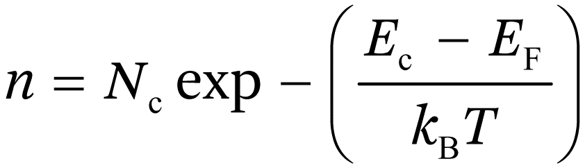
The semiconductor in Figure 1.1 is doped n-type by the presence in the crystal lattice of donor atoms that can be ionized at room temperature, releasing electrons to vacant levels in the conduction band. The concentration of electrons in the conduction band under conditions of thermal equilibrium is given by the Fermi–Dirac equation:
 (1.1a)
where Nc is the density of states in the conduction band. For normal levels of doping (<1018 cm−3), the exponential term in eqn (1.1a) is much larger than unity, so that the electron density can be approximated by the Boltzmann equation:
(1.1a)
where Nc is the density of states in the conduction band. For normal levels of doping (<1018 cm−3), the exponential term in eqn (1.1a) is much larger than unity, so that the electron density can be approximated by the Boltzmann equation:
 (1.1b)
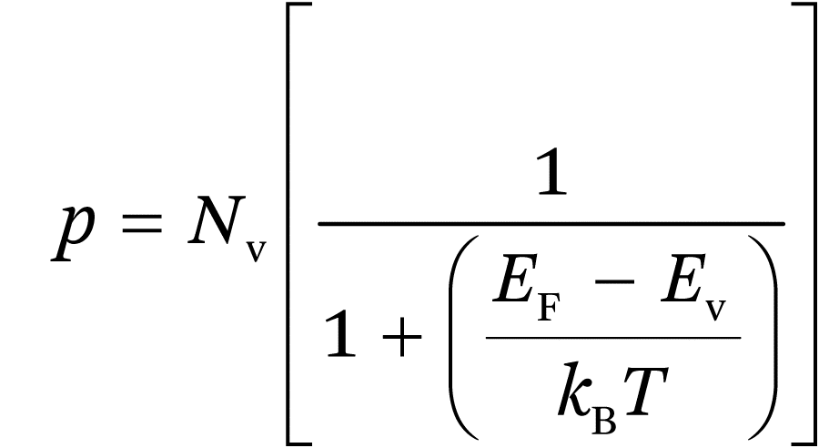
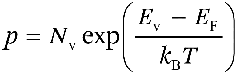
It follows that the Fermi energy shown in Figure 1.1 indicates the type and level of doping. The higher the n-doping, the closer EF is to the conduction band. In the case of p-type doping, electron acceptors in the crystal lattice accept electrons from the occupied valence band, creating holes. The concentration of holes under thermal equilibrium conditions is given by:
 (1.2a)
and for normal doping levels:
(1.2a)
and for normal doping levels:
 (1.2b)
It follows that the Fermi level in p-type semiconductors lies close to the valence band. Regardless of the type of doping, the product of the equilibrium concentrations of electrons and holes is given by the law of mass balance:
 (1.3)
where ni is the intrinsic electron density for the undoped case where electrons and holes are only produced by thermal excitation of electrons across the gap, so that n = p.
(1.3)
where ni is the intrinsic electron density for the undoped case where electrons and holes are only produced by thermal excitation of electrons across the gap, so that n = p.
Notably, EF is equivalent to the electrochemical potential of electrons. This means that it is a free energy that depends not only on concentration (via the temperature × entropy term in the Gibbs free energy G = U + PV − TS) but also on electrical potential. By contrast, Ec and Ev are internal energy terms that correspond to the standard states for electrons and holes, respectively. For a lucid discussion of the thermodynamics of the Fermi energy, the reader is referred to the excellent book by Würfel.12
1.3 Conventional Semiconductor Photoelectrodes
Early work on semiconductor electrodes focussed on the elemental semiconductors silicon and germanium. However, these elements are unstable in contact with water, forming surface oxide or hydroxide layers that complicate their electrochemical behaviour, so that progress was slow. The first semiconductor electrode that was found to behave almost ideally in aqueous solution was monocrystalline n-type ZnO,13 which can be prepared by chemical etching to expose well-defined stable polar faces with a low density of defects. Even today, ZnO remains one of the best-behaved semiconductor electrodes in terms of the potential distribution across the solid/electrolyte interface. The reason for this is that it can be prepared with a very low density of surface states. These are states associated with defects or impurities that can store electronic charge, altering the potential distribution. Indeed, if the density of surface states is very high, semiconductor electrodes may behave more like metal electrodes. It is important to realize that non-ideal behaviour is unfortunately the norm for most semiconductor electrodes, even if they are monocrystalline. Care is therefore needed in applying some of the simple models developed in the next sections.
1.3.1 Potential and Charge Distribution Across the Semiconductor–Inert Electrolyte Junction
Here we review briefly some essential concepts that are applicable in the case of an ideal semiconductor surface (i.e. one free of surface states) that is immersed in an electrolyte. The situation where a semiconductor is in contact with an inert electrolyte (i.e. one not containing any redox system) in the dark is the simplest to describe. We therefore begin by considering an n-type electrode like ZnO in contact with an electrolyte with a well-defined pH (for a p-type semiconductor, the signs of the charges and consequently the direction of band bending are reversed). The potential of the electrode can be controlled with respect to a reference electrode using a potentiostat, and if no interfacial electron transfer takes place, the electrode behaves as a capacitor. A convenient reference point for describing the potential and charge distribution across the junction is the flat-band potential, Ufb. This is the electrode potential at which there is no excess charge on the semiconductor side of the junction. This means that the number of electrons is exactly matched by the number of ionized donor atoms (remember that n-type doping is achieved by adding donor atoms that can ionize readily to supply electrons to the conduction band, leaving immobile donor ions D+ in the lattice). Because there is no excess charge in the semiconductor, there is no also electrical field. Now if the potential is made more positive than Ufb, electrons are withdrawn from the electrode (depletion condition), leaving a positive space charge region consisting of the ionized donor atoms. The width of the space charge region, Wsc, depends on the doping density, Nd, the relative permittivity, ε, and the potential drop across the space charge region, Δϕsc:
 (1.4)
(1.4)
The existence of a uniform positive space charge generates an electric field that varies linearly with distance from x = Wsc to x = 0 (the surface) (Figure 1.2). This linear variation of electric field corresponds to a variation of electrical potential that is parabolic (i.e. proportional to x2). This variation of potential across the space charge region changes the energy of electrons and holes and is reflected in the band bending shown in Figure 1.2.

The positive charge in the space charge region in the semiconductor is balanced by a net charge of opposite sign in the electrolyte created by rearrangement of ions. For concentrated electrolytes, this charge is effectively located at the outer Helmholtz plane of the electrical double layer. The overall charge distribution across the semiconductor–electrolyte junction that results is illustrated in Figure 1.2. It can be seen that the majority of the potential drop across the semiconductor–electrolyte interface occurs in the space charge region. For example, in the case of a doping density of 1017 cm−3 and a band bending of 0.5 eV, >99% of the potential drop across the interface occurs in the space charge region (it is important to note that the situation is different for semiconductors with surface states that can store electronic charge – see Section 1.5). The Fermi energy is constant across the space charge region and current flow is negligible. Since the electron concentration is given by eqn (1.1), it can be seen that the equilibrium electron concentration at the surface is orders of magnitude lower than in the bulk of the semiconductor, hence the term depletion.
The variation of the space charge (Qsc) with the potential drop (Δϕsc) across the space charge region defines the space charge capacitance, Csc = dQsc/dΔϕsc. The dependence of Csc on Δϕsc is given by the Mott–Schottky equation (here for an n-type electrode):
 (1.5)
(1.5)
The space charge capacitance appears in series with the Helmholtz capacitance, which is determined by the permittivity and width of the Helmholtz layer:
 (1.6)
(1.6)
The capacitance of the Helmholtz layer is expected to lie in the range 20–100 µF cm−2. These values are usually much higher than Csc under depletion conditions, and so for low or moderately doped semiconductors it is often assumed that changes in electrode potential appear mainly across the space charge region. In this case, Δϕsc in eqn (1.5) can be replaced by U − Ufb, where U is the applied potential. However, for many of the materials that are currently of interest, for example in the context of water splitting, this approximation may not be valid for several reasons. Firstly, Csc may be comparable with CH if the material is doped to levels above 1018 cm−3, as is often the case for non-stoichiometric oxides. Secondly, the derivation of eqn (1.5) involves an assumption that no electronic charge is stored at the surface of the semiconductor (no surface states).
Capacitance–voltage measurements are widely used to determine the flat band potential and doping density of semiconductors. Plots of 1/Csc2versus electrode potential are expected to be straight lines with slopes that are inversely proportional to the doping density (cf.eqn (1.5)). If CH ≫ Csc, the intercept gives the value of Ufb − kBT/q. However, if the doping density is high, a correction needs to be made for the Helmholtz capacitance.14 This is particularly important for materials with very high relative permittivity (e.g. rutile).
The potential drop across the Helmholtz layer is also sensitive to the ionic surface charge on the semiconductor. Acid/base equilibria for surface groups on oxide semiconductors give rise to a Nernstian pH dependence of the flat band potential, which shifts negative by 59 mV per pH unit at room temperature: Ufb = Ufb(pH0) − 0.059pH (1.7)
The flat band potential of chalcogenide semiconductors (e.g. CdS) depends in a similar way on the concentration of chalcogenide ion (e.g. HS−) in the solution as well as on pH, although the pH dependence is not Nernstian. Surface charge is also important in the case of colloidal semiconductors since it influences the position of the valence and conduction bands relative to solution redox levels. The surface dipole potential needs to be taken into account when relating flat band potentials (and hence the band energies) to the absolute energies shown in Figure 1.1. In this context, it is often assumed that the surface dipole associated with ionic species on the surface is negligible at the pH of zero charge, pHpzc. Further details can be found in a comprehensive review by Xu and Schoonen.15
1.3.2 The Semiconductor–Redox Electrolyte Junction
If a semiconductor is immersed in an electrolyte containing a redox couple, electronic equilibrium can be established between the two phases by electron transfer across the interface. The principles that govern the formation of such a semiconductor–redox electrolyte junction are the same as those that are applied to describe the junctions between n and p-type semiconductors and between semiconductors and metals. Electron exchange between the semiconductor and the electrolyte involves the reaction (for simplicity we consider a one-electron process): O + e− + R (1.8)
Since the electrochemical potential or Fermi level of electrons in both phases must be the same at equilibrium, the equilibrium condition for reaction (1.8) can be written in terms of the electrochemical potentials of the reactants and products:
![[small mu, Greek, macron]](./CHAPTER 1 Photoelectrochemistry_ From Basic Principles to Photocatalysis (RSC Publishing) DOI_10.1039_9781782622338-00001_files/i_char_e0cd.gif) o + n = R
(1.9)
o + n = R
(1.9)
It follows that n, the electrochemical potential of electrons in the semiconductor, is equal to the difference between the electrochemical potentials of R and O. Since the electrochemical potential of electrons is equivalent to the Fermi energy, this allows us to define a redox Fermi energy, EF,redox.16EF,redox depends on the standard reduction potential (Uo) of the O/R redox couple and on the concentrations of O and R (CO, CR).
The equilibrium redox potential on the standard hydrogen scale is given by the Nernst equation (n is the number of electrons transferred in the redox reaction):
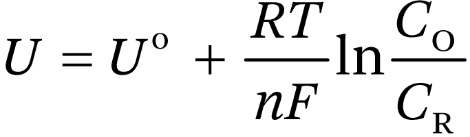 (1.10)
Taking the vacuum level as the zero energy, EF,redox is given by:
 (1.11)
where the standard reduction potential is measured on the standard hydrogen scale (SHE). Eqn (1.11) is based on a recommended estimation of the position of the H+/H2 redox Fermi level as −4.44 eV on the vacuum scale17 as illustrated in Figure 1.3. The figure also shows the valence and conduction band energies for CdS, Fe2O3 and TiO2 calculated for the respective pH values where the surface charge is zero (pHpzc) so that the ionic surface dipole is zero.15
(1.11)
where the standard reduction potential is measured on the standard hydrogen scale (SHE). Eqn (1.11) is based on a recommended estimation of the position of the H+/H2 redox Fermi level as −4.44 eV on the vacuum scale17 as illustrated in Figure 1.3. The figure also shows the valence and conduction band energies for CdS, Fe2O3 and TiO2 calculated for the respective pH values where the surface charge is zero (pHpzc) so that the ionic surface dipole is zero.15

The concept of a Fermi level in a phase that is not electronically conducting might seem odd at first, but it arises naturally from the equilibrium condition. However, electrons in the electrolyte phase are not free to move as they are in the semiconductor. Instead they are localized on redox ions. In effect, the occupied state is R and the empty state is O. These two states have different charges and hence different energies as a consequence of interactions with the solvent. In fact, the electronic energies of the two states change rapidly with time due to fluctuations of the solvent dipoles. The fluctuating energy model is the basis of the Marcus theory of outer sphere electron transfer.18 The fluctuating energy levels can be represented by the Gaussian probability functions, W(E) shown in Figure 1.4. For equal concentrations of O and R (i.e. standard conditions), the probability distributions have the same maximum value. The redox Fermi level is located at the intersection between the distribution curves, and electron transfer involves fluctuation of the energy from the most probable value represented by the peaks in the distributions to the iso-energetic crossing point, so that it is a thermally activated process. The kinetics of electron transfer therefore depend on how broad the distributions are: this is determined by the reorganization energy. Further details can be found in the literature.19,20

The relative positions of the Fermi levels in the semiconductor and in the redox electrolyte determine what happens when the two are brought into contact. If we consider an n-type semiconductor immersed in a redox electrolyte that has a redox Fermi level that lies below the Fermi level in the solid, electrons will be transferred to the oxidized species in solution until equilibrium is reached. This transfer of charge leads to the formation of a depletion layer (i.e. a space charge layer due to removal of electrons) in the semiconductor (Figure 1.5). Note that the Fermi levels in both phases must be equal at equilibrium. The band bending produced by the equilibration is determined by the difference between the two Fermi levels shown on the left-hand side of the figure. A very similar band diagram results if a semiconductor is contacted with a metal with a higher work function. The band diagram shows that there is a high barrier for electrons moving from the reduced species R to the conduction band. This is referred to as the Schottky barrier. If the potential is biased from equilibrium to more negative values, the band bending decreases and current begins to flow as electrons move from the conduction band into the electrolyte, resulting in reduction of the oxidized species. However, if the potential of the semiconductor is biased to more positive values, the Schottky barrier limits electron transfer from the electrolyte to the conduction band, so that only a very small current (the reverse saturation current) flows corresponding to oxidation of R by thermal excitation of electrons into the conduction band of the electrode. The junction therefore behaves as a Schottky diode, blocking current flow in one direction.

1.3.3 The Semiconductor–Electrolyte Junction Under Illumination
When a semiconductor absorbs photons with energy hν > Egap, electrons are excited from the valence band to vacant states in the conduction band, creating electron–hole pairs. We consider now what happens if the semiconductor is initially in equilibrium with a redox electrolyte in the dark so that the bands are bent as shown in Figure 1.5. The holes that are created by illumination can accept electrons from the reduced redox species, bringing about an oxidation reaction: R + h+ = O (1.12)
Since the concentration of holes in the dark is much smaller than the concentration of electrons in the case of an n-type semiconductor, the hole is referred to as the minority carrier, and reaction (1.12) represents a minority carrier reaction. It follows that, whereas oxidation in the dark is prevented by the high barrier for transfer of electrons from R to the conduction band (an endo-energetic process), oxidation becomes easy under illumination since electrons are transferred to the holes in the valence band (an exo-energetic process).
The hole in an n-type semiconductor is a metastable species since electrons can pass from the conduction band to the valence band. This is the process of electron–hole recombination. In the bulk of the semiconductor where the electron concentration is high (n ≫ p), recombination is a fast pseudo-first order process characterized by a lifetime τp that can range from milliseconds for ultra-pure silicon down to nanoseconds or less for many of the materials used in photocatalysis. The finite lifetime of the minority charge carrier imposes limits on the efficiency of reaction (1.12) in terms of the fraction of the absorbed photon flux that is converted into a current. To derive an expression for the external quantum efficiency (EQE) or incident photon to current efficiency (IPCE), we consider the three regions of the junction shown in Figure 1.6.

The incident photon flux I0 is attenuated as light enters the semiconductor, so that the rate of photon absorption, and hence the rate of electron–hole pair generation G(x), at any point is given by: G(x) = α(λ)I0exp[−α(λ)x] (1.13) where I0 is the incident photon flux, α(λ) is the wavelength-dependent absorption coefficient and x is the distance measured from the interface into the semiconductor.
The electrical field in the bulk region of the semiconductor is very small, and the concentration of majority carriers (electrons in the case of an n-type electrode) is determined by the doping density. Minority carriers (holes in the n-type case) in this region diffuse a certain distance before recombining. The minority carrier diffusion length, Lmin, is given by:
 (1.14)
where Dmin is the diffusion coefficient, τmin is the bulk lifetime and µmin is the mobility of minority carriers.
(1.14)
where Dmin is the diffusion coefficient, τmin is the bulk lifetime and µmin is the mobility of minority carriers.
The electrical field in the space charge region increases towards the surface as shown in Figure 1.2, and the equilibrium majority carrier concentration falls rapidly as the band bending qΔϕsc increases. In the n-type case illustrated in Figure 1.5, the electron concentration at the surface is given by:
 (1.15)
The probability of electron–hole pairs separating successfully is therefore much higher in the space charge region, and if the minority carriers react rapidly when they reach the interface, one can assume that electron–hole separation is 100% efficient in the space charge region. In addition, minority carriers that reach the edge of the space charge region by diffusion are likely to be transferred to the interface, so electron–hole separation extends beyond the edge of the space charge region by a distance that depends on the diffusion length defined in eqn (1.14). This boundary value problem was first solved for the analogous solid-state junction by Gärtner.21 The IPCE, which is the ratio of the measured electron flux (Jn) in the external circuit to the incident photon flux is given by the Gärtner equation, which can be expressed in terms of the photocurrent density (jphoto) in the form:
 (1.16)
The derivation of the Gärtner equation assumes that minority carriers are transferred rapidly across the interface. This is certainly the case for a solid state junction, but in the case of the semiconductor–electrolyte interface, electron transfer is thermally activated. The Gärtner equation still applies provided that a fast outer sphere redox system is used as the electrolyte. However, if electron transfer is slow, minority carriers will build up in the space charge region, changing the band bending and promoting recombination. This is likely to be the case for slow multistep reactions such as those involved in the oxidation of water at n-type photoelectrodes (photoelectrolysis). In such cases, the IPCE can be much lower than the values predicted by the Gärtner equation because electron–hole pairs recombine in the space charge region as well as in the neutral bulk region.
1.3.4 Quasi-Fermi Levels (QFLs)
The Fermi level concept can be extended from equilibrium (dark) systems to systems under steady state illumination where the electron and hole concentrations differ from their equilibrium values. Since photoexcited electrons and holes equilibrate with lattice phonons in less than 10−12 s, whereas electron–hole recombination generally occurs on a timescale >10−9 s, one can assume that electrons and holes are in thermal equilibrium with the lattice, but not with each other. This allows us to define quasi Fermi levels (QFLs) for electrons and holes, which are given by:
 (1.17a)
 (1.17b)
where n and p are photostationary electron and hole concentrations. The QFL concept is widely used in semiconductor physics and is particularly useful for the description of photovoltaic cells (see, for example, Würfel12 for details). In principle, the profiles of electron and hole concentrations can be obtained by solving the continuity equations for transport, recombination and interfacial electron transfer with appropriate boundary conditions,22–24 but more frequently the QFLs are simply sketched to illustrate basic principles. Reineke and Memming25 used the QFL concept to compare the photocurrents measured at n-type electrodes with the currents measured in the dark for a p-type electrode of the same material. They were able to show that the rates of electron transfer were determined only by the (quasi)Fermi level position relative to the redox Femi level. Recently Cendula et al.26 have provided a useful summary of basic concepts and have calculated QFL profiles for very thin films of n-Fe2O3 and p-Cu2O by making the simplifying assumption that illumination does not change the majority carrier Fermi level significantly (low injection conditions). Figure 1.7 illustrates the general features of the QFL profiles at an illuminated junction between an n-type semiconductor and an electrolyte.
(1.17b)
where n and p are photostationary electron and hole concentrations. The QFL concept is widely used in semiconductor physics and is particularly useful for the description of photovoltaic cells (see, for example, Würfel12 for details). In principle, the profiles of electron and hole concentrations can be obtained by solving the continuity equations for transport, recombination and interfacial electron transfer with appropriate boundary conditions,22–24 but more frequently the QFLs are simply sketched to illustrate basic principles. Reineke and Memming25 used the QFL concept to compare the photocurrents measured at n-type electrodes with the currents measured in the dark for a p-type electrode of the same material. They were able to show that the rates of electron transfer were determined only by the (quasi)Fermi level position relative to the redox Femi level. Recently Cendula et al.26 have provided a useful summary of basic concepts and have calculated QFL profiles for very thin films of n-Fe2O3 and p-Cu2O by making the simplifying assumption that illumination does not change the majority carrier Fermi level significantly (low injection conditions). Figure 1.7 illustrates the general features of the QFL profiles at an illuminated junction between an n-type semiconductor and an electrolyte.

The minority carrier QFL at the surface of an n-type photoelectrode in contact with a redox electrolyte is determined by the rate constant for electron transfer to the hole from the reduced species. The rate (and hence the current density) of interfacial electron transfer can be written in terms of the number concentrations of reactants (holes and R in our case) at the surface: jphoto = qket[px = 0][R] (1.18)
For fast outer sphere reactions, ket is expected to be of the order of 10−18 cm−3 s−1.27 If we consider, for the purposes of illustration, a photocurrent density of 1 mA cm−2 and a redox concentration [R] = 0.1 M (6 × 1019 cm−3), the concentration of holes at the surface will be ca. 1014 cm−3. If the effective density of states in the valence band (Nv) is 1019 cm−3, the hole QFL will be ca. 300 meV above Ev at the surface as illustrated in Figure 1.7. If, on the other hand, electron transfer is very slow, the hole QFL may approach or even enter the valence band energy due to the build-up of holes at the surface.28 This build-up of holes will substantially modify the potential distribution across the junction, lowering the band bending and increasing the potential drop across the Helmholtz layer.
1.4 Nanostructured Semiconductor Electrodes and Colloidal Particles in the Dark
1.4.1 Band Bending in Nanostructures
Nanostructured and mesoporous electrodes differ in several important respects from the flat surfaces described in the preceding sections. Firstly, the characteristic length scale of the nanostructured electrode may be compared with the Debye length, LD, which is given by:
 (1.19)
where N is the dopant concentration. If the lengths scales of the particles that make up the nanostructure are smaller than LD, it is not possible to develop substantial band bending. This can be illustrated for the case of a spherical semiconductor particle of a doped semiconductor. The radial distribution of electrical potential in a spherical particle was derived by Albery and Bartlett.29 If the particle radius r0 is much smaller than the depletion width, the potential profile reduces to the simple parabolic form:
(1.19)
where N is the dopant concentration. If the lengths scales of the particles that make up the nanostructure are smaller than LD, it is not possible to develop substantial band bending. This can be illustrated for the case of a spherical semiconductor particle of a doped semiconductor. The radial distribution of electrical potential in a spherical particle was derived by Albery and Bartlett.29 If the particle radius r0 is much smaller than the depletion width, the potential profile reduces to the simple parabolic form:
 (1.20)
To illustrate the effect of size on band bending, we can consider a 50 nm diameter fully depleted anatase particle with a doping density of 1017 cm−3 and a relative permittivity of 30. As Figure 1.8 shows, the maximum band bending in this case is only around 13 meV. Increasing the doping density to 1018 cm−3 allows the development of higher band bending: now saturation occurs at a band bending ten times higher. In the first case, the band bending is smaller than the average thermal energy kBT, so the effects of the band bending on charge carrier distributions can be neglected. In the second case, the band bending is large enough to affect the distribution of electrons and holes in the particle.

The potential drop ΔVH across the Helmholtz layer can be calculated for the two cases shown in Figure 1.8 using the principle of dielectric continuity. The ΔVH values are 0.6 and 6 mV for doping levels of 1017 and 1018 cm−3, respectively.
Similar considerations regarding band bending apply to other nanostructured electrodes such as nanorods or nanotubes: in this case it is the smallest characteristic dimension that is relevant. If the nanostructured electrode has a more complex structure, then small features may be almost field-free, whereas significant electrical fields will be present in the space charge region that can be developed in larger features. In the case of vertically aligned nanorods, for example, the answer to the question of whether they have a significant electrical field normal to the long axis will depend on their size and doping density. In the case of highly doped nanorods, separation of electron–hole pairs may be assisted by the electrical field, provided that the rod radius is larger than Wsc. Less regular nanostructured systems composed of structures with different characteristic length scales will require numerical 3D modelling. The remarks regarding band bending outlined here are relevant to colloidal systems used for photocatalysis. However, determination of the doping density is often difficult or impossible for dispersed colloidal systems, so that it is not easy to decide whether band bending effects are important.
In the preceding discussion it was assumed that the potential of the semiconductor electrode could be controlled by a potentiostat. If we are dealing with a suspension of nanoscale semiconductor particles in a redox electrolyte (in the dark), the position of the Fermi level will be determined by the redox Fermi level, which depends on the concentrations of oxidized and reduced species according to the Nernst equation (cf.eqn (1.11)). If a colloidal TiO2 particle is immersed in a redox electrolyte, the Fermi levels of the two phases will equilibrate in the dark by electron exchange. To illustrate some basic principles, we consider two cases. The first example is an I3−/I− electrolyte at pH 7 under standard conditions (CO = CR). At pH 7, the redox Fermi level of the I3−/I− couple lies about 1.0 eV below the Fermi level of the unperturbed TiO2. Consequently, for typical particle sizes (5–20 nm diameter), the TiO2 particles will be completely depleted of electrons because the Fermi level will be pulled down to around 1.0 eV below the conduction band. Calculation of the equilibrium electron concentration using eqn (1.1b) gives values below 103 cm−3. This means that there is a chance of around one in a billion of finding even a single electron in a TiO2 particle in the dark. Contrast this with a TiO2 particle immersed in a methylviologen redox electrolyte MV2+/MV+˙ (CO = CR) at pH 7, where the Fermi level in the electrolyte is close to the conduction band of the TiO2. Equilibration will push the electron Fermi level close to the conduction band of the TiO2 so that each particle will contain 100 or more electrons.
1.4.2 Determination of Quasi-Fermi Level Positions in Nanoparticle Suspensions
Since capacitance measurements are not feasible for dispersed nanoparticles, determination of the energetics of the nanoparticle/electrolyte interface requires different methods. Ward et al.30 showed that the Fermi energy for TiO2 particle suspensions could be determined as a function of pH by using a platinum collector electrode to measure photocurrents in stirred deoxygenated TiO2 (anatase) suspensions under illumination. The method involves using an acetate buffer to remove photogenerated holes from the particles and methylviologen MV2+ as an electron-trapping agent. The irreversible photo-oxidation of acetate (the photo Kolbe reaction) removes holes rapidly, leaving the photogenerated electrons to reduce MV2+ to MV+˙: 2CH3COO− + 2h+ = 2CO2 + C2H6 (1.21a) 2MV2+ + 2e− = 2MV+˙ (1.21b)
For reaction (1.21b) to proceed rapidly, the Fermi level of electrons in the TiO2 must be close to the standard reduction potential for the MV2+/MV+˙ couple as illustrated in Figure 1.9. The position of the TiO2 conduction band can be tuned by changing the pH (cf. Section 1.3.1). Increasing the pH moves the flat band potential to more negative values, which corresponds to moving the band energies upwards relative to a pH-independent redox Fermi level. The standard reduction potential of the MV2+/MV+˙ couple is −0.45 V vs. SHE, and the photocurrent onset corresponding to the detection of significant amounts of the radical cation in the solution occurs at pH 6.7. If we assume that the Fermi level in the TiO2 is aligned with the methylviologen redox Fermi level at this pH, then the flat-band potential at pH 6.7 is −0.45 V vs. SHE. Taking into account the pH dependence of Ufb therefore gives Ufb (pH 0) = −0.05 V vs. SHE, which is in good agreement with values for bulk TiO2. The same system was studied by Dung et al.,31 who detected the blue MV+˙ radical cation by absorption spectroscopy and obtained a more negative flat-band potential (Ufb = −0.15 V vs. SHE) for TiO2 (anatase). The methylviologen/pH method has also been used to determine the flat-band potential of colloidal CdS with potentiometric detection of the formation of the radical cation,32,33 although here the variation of flat-band potential with pH is not Nernstian.

1.5 Surface States and Fermi Level Pinning
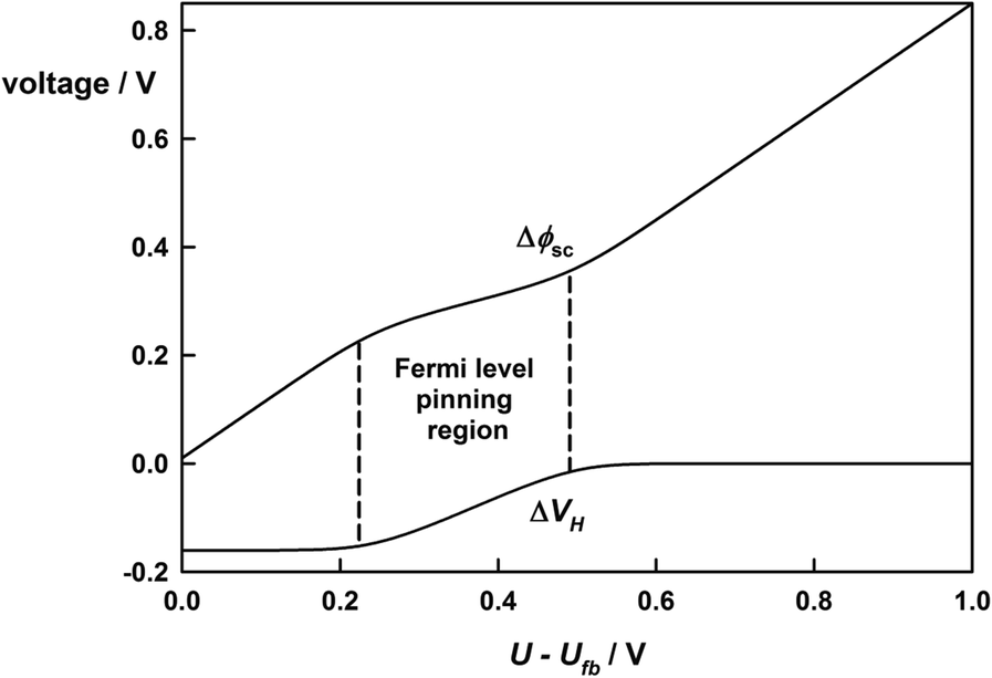
Very few semiconductor–electrolyte junctions behave ideally. The primary reason is that the surface of a semiconductor represents a discontinuity in the lattice that can give rise to electronic energy levels associated with ‘dangling bonds’ or with termination of the lattice by some form of chemical binding to solutions species. These electronic energy levels are termed surface states, and because they are able to exchange electrons with the bulk semiconductor and with redox species in solution they alter the potential distribution across the junction. This effect can be illustrated by considering the idealized case of a mono-energetic surface state located in the bandgap of the semiconductor. The surface state is characterized by a particular energy (Ess) and surface concentration, Nss. The occupation of the surface state energy levels is determined by the position of the Fermi level in the semiconductor as illustrated in Figure 1.10 for an n-type semiconductor with a surface state energy level near the conduction band. Initially the Fermi level lies above Ess so the surface states are occupied by electrons, as the electrode potential is made more positive, the Fermi level moves downwards until it coincides with Ess. Further positive biasing of the electrode results in the surface states being emptied of electrons and finally when the Fermi level is below Ess, the surface states are empty.

The transition in electron occupation of the surface states from filled to empty corresponds to a change in surface charge equal to qNss. This gives rise to a change in the potential drop across the Helmholtz layer:
 (1.22)
This means that when the Fermi level reaches Ess, further changes in potential appear across the Helmholtz layer until all electrons have been removed from the surface states. While this change is taking place, the potential drop in the semiconductor – and hence the band bending – varies much more slowly with applied voltage. In essence the Fermi level has become ‘stuck’ in the surface state. This phenomenon is referred to as Fermi level pinning.34,35 An alternative term is band edge unpinning. This term reflects the fact that the band energies of a semiconductor electrode are normally fixed relative to redox energy levels, whereas the band edges shift if the potential drop across the Helmholtz layer changes as a consequence of surface state charging. Figure 1.11 illustrates the consequences of surface state charging for the potential distribution across the junction.
1.6 Surface Recombination
Ultimately the quantum efficiency of any photoelectrochemical or photocatalytic process depends on the competition between the desired reaction on the one hand and loss of photogenerated carriers by recombination on the other. So far, we have only considered recombination in the bulk of a semiconductor. This can occur by direct band to band electron transfer or, more commonly, via defect or impurity states in the forbidden gap. For semiconductor–electrolyte junctions we can distinguish between bulk recombination and recombination in the space charge region. However, it is important to realize that electron–hole recombination can also occur via surface states (surface recombination36–39), and clearly this pathway will be particularly important for systems such as nanostructured electrodes or suspensions of nanoparticles or colloids with very high surface area to volume ratios.
Surface recombination seems to be the most important loss mechanism for many semiconductor photoelectrodes, but the exact nature of the states involved is not always clear. In some cases, the presence of surface states can be related to surface preparation. For example, mechanical polishing of single crystal photoelectrodes generates high densities of defects that act as surface states.40 These can be removed by chemical etching. However, even carefully prepared single crystal semiconductor surfaces exhibit surface recombination. A notable exception is the hydrogen-terminated (111) surface of silicon obtained by etching in HF,41 which is almost entirely free of surface states.
Surface states may also be involved in charge transfer to the electrolyte, giving rise to the competition pathways outlined in Figure 1.12. A simple model based on this scheme has been used to predict the time and frequency-dependent photocurrent response of semiconductor electrodes.42,43 If we neglect direct charge transfer from the valence band, the efficiency of the charge transfer process involving oxidation of solution species can be formulated in terms of the rates of the competing processes involving the surface concentration of trapped holes, psurf:
 (1.23)
where ktrans and krec are first order rate constants for charge transfer and recombination respectively. The recombination rate constant (krec) depends on the concentration of electrons at the surface (cf.eqn (1.15)), and so increasing the band bending decreases recombination. Generally speaking, charge transfer to outer sphere redox systems is sufficiently fast that recombination can be neglected. However, if charge transfer is slow because it involves several steps such as those involved in oxygen evolution, for example, recombination leads to a delayed onset of photocurrent as a function of applied voltage. An alternative to using a fast redox system to obtain ‘ideal’ photocurrent voltage plots is to use a hole scavenger that reacts rapidly and irreversibly. A good example is the SO32− ion, which is oxidized irreversibly to SO42− by photogenerated holes.
(1.23)
where ktrans and krec are first order rate constants for charge transfer and recombination respectively. The recombination rate constant (krec) depends on the concentration of electrons at the surface (cf.eqn (1.15)), and so increasing the band bending decreases recombination. Generally speaking, charge transfer to outer sphere redox systems is sufficiently fast that recombination can be neglected. However, if charge transfer is slow because it involves several steps such as those involved in oxygen evolution, for example, recombination leads to a delayed onset of photocurrent as a function of applied voltage. An alternative to using a fast redox system to obtain ‘ideal’ photocurrent voltage plots is to use a hole scavenger that reacts rapidly and irreversibly. A good example is the SO32− ion, which is oxidized irreversibly to SO42− by photogenerated holes.
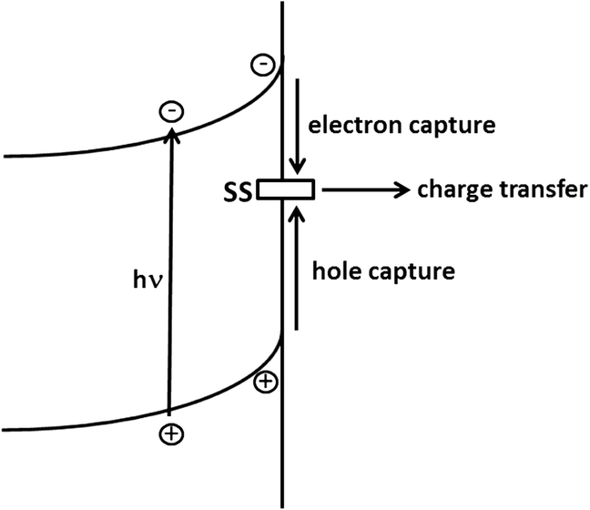
An interesting question is whether the surface states in which holes are trapped exist in the dark. All that is required in the scheme shown in Figure 1.12 is that the hole should be located in a surface energy level in the gap. In fact the ‘surface-trapped hole’ may have a distinct chemical identity as a result of interactions between the semiconductor and the solution. So, for example, the trapping of a hole could involve formation of a surface bound species by a reaction such as: H2O + h+ = H+ + OHads (1.24)
In this case the trapped hole is in fact an intermediate in the oxidation of water to dioxygen, which overall is a four-hole process: 2H2O + 4h+ = 4H+ + O2 (1.25)
The ‘chemical’ identity of the surface trapped hole is therefore a topic of considerable interest in the context of light-driven water splitting and, of course, photosynthetic and photocatalytic reactions at colloidal semiconductors.
The accumulation of surface-trapped holes or photogenerated intermediates at the surface can lead to Fermi level pinning. The effects will be particularly evident at high light intensities and for slow charge transfer. Fermi level pinning exacerbates the effects of surface recombination, explaining the highly non-ideal photocurrent–voltage response of many photoelectrodes used for light-driven water splitting.
The situation with uncontacted semiconductor nanoparticles is similar. In this case, the net current flow across the interface of the particle must be zero under photostationary conditions since there is no external connection. If, for example, an electron scavenger, A, is used, photogenerated electrons will initially be removed preferentially, leaving holes that react more slowly with an electron donor, D, in the solution (e.g. with water to form oxygen). In the photostationary state the flux balance for electrons and holes will be given by:
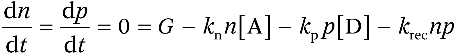 (1.26)
where G is the rate of generation of electron–hole pairs by absorbed photons and the last term represents electron–hole recombination. If kn ≫ kp, the concentration of holes will build up in the illuminated particle, and if they are trapped at the surface (or if they react to form surface-bound intermediates), there will be a change in the potential drop across the Helmholtz layer and band edge unpinning.
(1.26)
where G is the rate of generation of electron–hole pairs by absorbed photons and the last term represents electron–hole recombination. If kn ≫ kp, the concentration of holes will build up in the illuminated particle, and if they are trapped at the surface (or if they react to form surface-bound intermediates), there will be a change in the potential drop across the Helmholtz layer and band edge unpinning.
1.7 Charge Compensation and Charge Trapping in Mesoporous Electrodes
So far we have only considered electrons and holes in the conduction and valence bands or in surface states. Mesoporous electrodes consisting of interconnected nanoparticles behave in a way that is quite different from their bulk counterparts. The most studied system is mesoporous anatase (TiO2), which is used in the dye-sensitized solar cell.9,44,45 Porous silicon has also been widely studied.46 In both cases the properties of the ‘dry’ electrode and the electrode permeated with an electrolyte are completely different. The presence of the ionic solution in the pores of the electrode allows very efficient screening of charges injected into the solid from the contacts. The very high electron concentrations that can be obtained can push the Fermi level into the conduction band. The accumulation of electrons can be detected optically, and this has been used to determine the position of the conduction band in mesoporous TiO2.47 By contrast, the ‘dry’ electrodes are essentially insulators. Polar molecules can also shield injected charges, and the changes in charge accumulation that result from the adsorption of polar substances from the gas phase is the basis for chemical sensing using mesoporous materials.48
Charge accumulation in mesoporous electrodes is not restricted to the conduction band. Mesoporous materials such as anatase and ZnO appear to contain extraordinarily high concentrations of electron traps – energy levels are distributed across the forbidden gap.49 These trap levels exert a strong influence on the speed of photocurrent and photovoltage responses of dye-sensitized solar cells because free electrons in the conduction band are exchanged with those in trap states. The trapped electronic charge can be detected by near-infrared absorption measurements50 or by a technique known as charge extraction.51,52 Interestingly, such high trap densities (>1019 cm−3) are only observed in nanocrystal systems with very small sizes (in the range 10–30 nm). At present the origin of the traps is not clear, but they appear to be associated with the surface rather than the bulk. This raises the interesting question of whether dispersed nanocrystals also have such high trap densities. In principle, one would expect this to be the case.
1.8 Conclusions
This brief overview of semiconductor electrochemistry has focussed on basic concepts rather than on materials. It is important to realize that very few materials behave ideally, so that care is needed when applying the concepts and methodologies outlined in this chapter. Wherever possible, chemical or electrochemical methods should be supported by other techniques, such as in situ spectroscopy, to obtain a fuller picture of a particular system. Unfortunately the properties of many materials are not very reproducible, so that results may depend strongly on sample preparation. The trend towards increasing complexity brought about by a strong emphasis on nanostructured electrodes may obscure some of the basic physical and chemical processes. In such cases, the use of well-defined flat surfaces may offer the best way forward in terms of understanding. Systems consisting of dispersed nanocrystals bring new challenges associated with their high surface area to volume ratio and the fact that at least two reactions are occurring on each particle to balance charge. Often the description of photo-induced processes at nanocrystals is oversimplified because too little is known about the role of bulk and surface defects. Progress in this area could be stimulated by closer examination of the parallels and differences between dispersions and mesoporous electrodes of the same material (cf. the discussion in the previous section regarding traps). Clearly, more remains to be done to adapt the basic principles of semiconductor electrochemistry to describe in more detail the behaviour of the disperse systems used in photocatalysis and photosynthesis.
References
-
H. Gerischer
Advances in Electrochemistry and Electrochemical Engineering
, P. DelahayInterscience, New York, 1961, vol. vol. 1, pp. 139–232
Search PubMed
.
-
R. Memming
Semiconductor Electrochemistry
, Wiley VCH Verlag GmbH, Weinheim, 2001,
Search PubMed
-
Encyclopedia of Electrochemistry Vol. 6, Semiconductor Electrodes and Photoeletrochemistry
, A. J. Bard, M. Stratmann and S. Licht, Wiley VCH Verlag GmbH, Weinheim, 2002,
Search PubMed
-
S. R. Morrison
Electrochemistry of Semiconductor and Metal Electrodes
, Plenum Press, New York, 1980,
Search PubMed
-
N. Sato
Electrochemistry at Metal and Semiconductor Electrodes
, Elsevier, Amsterdam, 1998,
Search PubMed
-
Y. V. Pleskov
and Y. Y. Gurevich
, Semiconductor Photoelectrochemistry
, Consultants Bureau, New York, 1985,
Search PubMed
-
Y. V. Pleskov
Solar Energy Conversion. A Photoelectrochemical Approach
, Springer, Berlin, 1990,
Search PubMed
-
A. Fujishima
and K. Honda
, Nature,
1972, 238
, 37
CrossRef
CAS
PubMed
-
B. O’Regan
and M. Grätzel
, Nature,
1991, 353
, 737
CrossRef
-
C. Kittel
Introduction to Solid State Physics
, John Wiley & Sons, Inc., Hoboken, 2005,
Search PubMed
-
N. W. Ashcroft
and N. D. Mermin
, Solid State Physics
, Holt Reinhart and Winston, 1976,
Search PubMed
-
P. Würfel
and U. Würfel
, Physics of Solar Cells. From Basic Principles to Advanced Concepts
, Wiley-VCH Verlag GmbH, Weinheim, 2009,
Search PubMed
-
J. F. Dewald
J. Phys. Chem. Solids,
1960, 14
, 155
CrossRef
CAS
-
R. De Gryse
, W. P. Gomes
, F. Cardon
and J. Vennik
, J. Electrochem. Soc.,
1975, 122
, 711
CrossRef
CAS
-
Y. Xu
and M. A. A. Schoonen
, Am. Mineral.,
2000, 85
, 653
Search PubMed
-
H. Gerischer
and W. Ekardt
, Appl. Phys. Lett.,
1983, 43
, 393
CrossRef
CAS
-
S. Trasatti
Pure Appl. Chem.,
1986, 58
, 955
CrossRef
CAS
-
R. A. Marcus
Annu. Rev. Phys. Chem.,
1964, 15
, 155
CrossRef
CAS
-
R. B. James
and D. A. Mary
, Electron Transfer in Inorganic, Organic, and Biological Systems
, American Chemical Society, Washington DC, 1991, vol. vol. 228, pp. 7–23
Search PubMed
-
A. M. Kuznetzov
and J. Ulstrup
, Electron Transfer in Chemistry and Biology: An Introduction to the Theory
, Wiley-Blackwell, 1998,
Search PubMed
-
W. W. Gärtner
Phys. Rev.,
1959, 116
, 84
CrossRef
-
F. El Guibaly
and K. Colbow
, J. Appl. Phys.,
1982, 53
, 1737
CrossRef
CAS
-
J. Reichman
Appl. Phys. Lett.,
1980, 36
, 574
CrossRef
CAS
-
M. J. Cass
, N. W. Duffy
, L. M. Peter
, S. R. Pennock
, S. Ushiroda
and A. B. Walker
, J. Phys. Chem. B,
2003, 107
, 5857
CrossRef
CAS
-
R. Reineke
and R. Memming
, J. Phys. Chem.,
1992, 96
, 1310
CrossRef
CAS
-
P. Cendula
, S. D. Tilley
, S. Gimenez
, J. Bisquert
, M. Schmid
, M. Grätzel
and J. O. Schumacher
, J. Phys. Chem. C,
2014, 118
, 29599
CrossRef
CAS
-
A. M. Fajardo
and N. S. Lewis
, J. Phys. Chem. B,
1997, 101
, 11136
CrossRef
CAS
-
L. M. Peter
J. Solid State Electrochem.,
2013, 17
, 315 —326
CrossRef
CAS
-
W. J. Albery
and P. N. Bartlett
, J. Electrochem. Soc.,
1984, 131
, 315
CrossRef
CAS
-
M. D. Ward
, J. R. White
and A. J. Bard
, J. Am. Chem. Soc.,
1983, 105
, 27
CrossRef
CAS
-
D. Dung
, J. Ramsden
and M. Graetzel
, J. Am. Chem. Soc.,
1982, 104
, 2977
CrossRef
CAS
-
D. Mitoraj
and H. Kisch
, J. Phys. Chem. C,
2009, 113
, 20890
CrossRef
CAS
-
A. M. Roy
, G. C. De
, N. Sasmal
and S. S. Bhattacharyya
, Int. J. Hydrogen Energy,
1995, 20
, 627
CrossRef
CAS
-
A. J. Bard
, A. B. Bocarsly
, F. R. F. Fan
, E. G. Walton
and M. S. Wrighton
, J. Am. Chem. Soc.,
1980, 102
, 3671
CrossRef
CAS
-
J. N. Chazalviel
and T. B. Truong
, J. Electroanal. Chem.,
1980, 114
, 299
CrossRef
CAS
-
H. Gerischer
J. Electroanal. Chem.,
1983, 150
, 553
CrossRef
CAS
-
J. Li
, R. Peat
and L. M. Peter
, J. Electroanal. Chem.,
1984, 165
, 41
CrossRef
CAS
-
J. Li
and L. M. Peter
, J. Electroanal. Chem.,
1985, 193
, 27
CrossRef
CAS
-
J. N. Chazalviel
J. Electrochem. Soc.,
1982, 129
, 963
CrossRef
CAS
-
H. Gerische
, F. Hein
, M. Lubke
, E. Meyer
, B. Pettinge
and H. R. Schoppel
, Ber. Bunsenges,
1973, 77
, 284
Search PubMed
-
E. Yablonovitch
, D. L. Allara
, C. C. Chang
, T. Gmitter
and T. B. Bright
, Phys. Rev. Lett.,
1986, 57
, 249
CrossRef
CAS
PubMed
-
E. A. Ponomarev
and L. M. Peter
, J. Electroanal. Chem.,
1995, 396
, 219
CrossRef
-
L. M. Peter
, E. A. Ponomarev
and D. J. Fermin
, J. Electroanal. Chem.,
1997, 427
, 79
CrossRef
CAS
-
L. M. Peter
Phys. Chem. Chem. Phys.,
2007, 9
, 2630
RSC
-
L. M. Peter
J. Phys. Chem. C,
2007, 111
, 6601
CrossRef
CAS
-
A. G. Cullis
, L. T. Canham
and P. D. J. Calcott
, J. Appl. Phys.,
1997, 82
, 909
CrossRef
CAS
-
G. Rothenberger
, D. Fitzmaurice
and M. Gratzel
, J. Phys. Chem.,
1992, 96
, 5983
CrossRef
CAS
-
I. Schechter
, M. Ben-Chorin
and A. Kux
, Anal. Chem.,
1995, 67
, 3727 —3732
CrossRef
CAS
-
L. Peter
Acc. Chem. Res.,
2009, 42
, 1839
CrossRef
CAS
PubMed
-
T. T. O. Nguyen
, L. M. Peter
and H. X. Wang
, J. Phys. Chem. C,
2009, 113
, 8532
CrossRef
CAS
-
N. W. Duffy
, L. M. Peter
, R. M. G. Rajapakse
and K. G. U. Wijayantha
, Electrochem. Commun.,
2000, 2
, 658
CrossRef
CAS
-
M. Bailes
, P. J. Cameron
, K. Lobato
and L. M. Peter
, J. Phys. Chem. B,
2005, 109
, 15429
CrossRef
CAS
PubMed
© The Royal Society of Chemistry 2016 (2016)